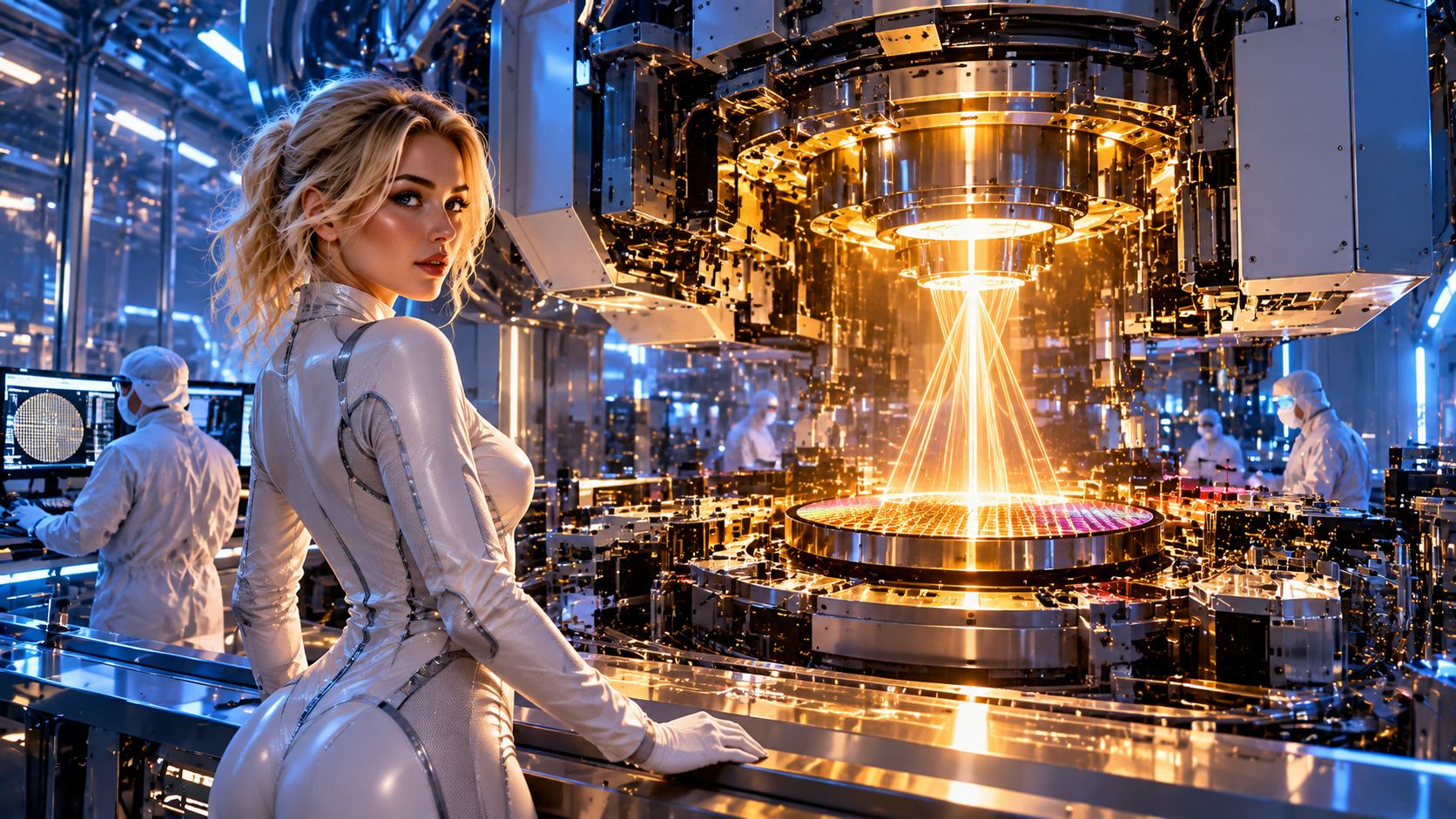
The world’s most advanced artificial intelligence systems depend on an industrial process that would look almost absurd to someone unfamiliar with semiconductor manufacturing. To produce the chips that train and run AI models, companies must operate enormous machines that fire lasers at microscopic droplets of molten tin, manipulate light using some of the most precisely manufactured mirrors on Earth, and build electrical structures one atomic layer at a time.
Those machines require other machines to manufacture their components. Their suppliers, in turn, depend on specialized optics, vacuum systems, industrial lasers, precision motion controls, ultra-pure materials and measuring instruments capable of detecting defects smaller than many viruses.
This is the industrial machinery business behind artificial intelligence, and it operates several layers beneath the companies most people associate with the AI boom.
Nvidia designs processors that have become central to AI computing. TSMC manufactures many of the world’s most advanced chips. But neither company could perform its role without an extensive network of semiconductor equipment manufacturers whose products turn extraordinarily difficult physics into repeatable industrial processes.
Some of these businesses are already substantial global corporations. Others are highly specialized suppliers whose names rarely appear in discussions about AI. Their commercial advantage often comes from decades of accumulated engineering expertise, intimate relationships with chipmakers and technologies that competitors cannot easily reproduce.
The deeper you travel into this supply chain, the stranger the business becomes. A company can hold an exceptionally important position in the AI economy without developing an AI model, designing a processor or operating a data center.
It may simply manufacture a component that makes another company’s machine possible.
Table of Contents
- The machines behind the AI machines
- ASML: The company that manufactures artificial sunlight
- The companies that make ASML’s machines possible
- The industrial giants that build chips atom by atom
- The businesses that find defects and test the finished chips
- Why selling semiconductor equipment is such an unusual business
- What the AI investment boom means for equipment suppliers
- The geopolitical problem hidden inside the machinery
- The industrial foundations of artificial intelligence
The machines behind the AI machines
The semiconductor industry has an unusual division of labor. A company such as Nvidia can design an advanced processor without owning the factories that manufacture it. A foundry such as TSMC can produce that processor using equipment purchased from specialized manufacturers. Those equipment manufacturers then source critical subsystems from an international network of industrial suppliers.
The distinction matters because chip design and chip manufacturing are fundamentally different activities.
Designing a modern processor involves determining how billions of transistors and their connections should be arranged. Manufacturing it requires reproducing that design on silicon wafers through hundreds of tightly controlled processing steps. The wafer repeatedly moves through equipment that deposits materials, creates patterns, removes selected portions of those materials, measures the results and prepares the surface for the next operation.
The process is closer to constructing an entire microscopic city than printing a conventional electronic circuit. Different materials must be positioned with extraordinary precision, often across multiple layers, while contamination and tiny variations can compromise the finished device.
A mistake in one critical operation can render an otherwise valuable chip unusable.
That creates a vast market for companies specializing in individual manufacturing problems. Some build lithography systems that transfer circuit patterns onto wafers. Others manufacture equipment for depositing thin films, etching microscopic structures, cleaning surfaces or measuring defects.
The resulting industry has its own hierarchy of global leaders, niche specialists and indispensable component suppliers.
For investors and technology enthusiasts accustomed to following Nvidia, AMD or the latest AI model, it is a very different world. Product cycles can stretch across years, customer relationships are unusually close, and a manufacturing improvement that sounds trivial outside the industry can be worth enormous sums.
A slightly faster machine, a cleaner process or a higher proportion of usable chips can materially change the economics of an entire semiconductor factory.
ASML: The company that manufactures artificial sunlight
The most spectacular example is ASML, the Dutch manufacturer of lithography equipment.
Lithography is the process used to transfer intricate patterns onto a silicon wafer. These patterns help define the transistors and interconnections that eventually become a functioning semiconductor.
As chip features have become smaller, conventional optical methods have encountered increasingly difficult physical limits. ASML’s answer has been extreme ultraviolet lithography, usually abbreviated to EUV.
EUV systems use light with a wavelength of approximately 13.5 nanometers. Producing and controlling that light requires an engineering arrangement unlike almost anything found in ordinary industrial machinery.
Inside the light source, tiny droplets of molten tin are struck by high-powered laser pulses. The interaction creates plasma that emits extreme ultraviolet radiation. Specialized mirrors then collect and guide the light toward the wafer.
Ordinary glass lenses cannot perform this job because EUV light is strongly absorbed by materials that are transparent to visible light. The optical system therefore relies on exceptionally precise reflective surfaces and operates in carefully controlled vacuum conditions.
A single lithography machine combines advanced optics, plasma physics, high-speed motion control, thermal management, software and extraordinary mechanical precision.
This is not equipment a competitor can replicate simply by hiring engineers and purchasing components.
ASML spent decades developing EUV technology with partners across several countries. Its machines are now central to manufacturing many of the most advanced semiconductor devices, including processors used for AI computing.
The financial scale is remarkable. According to its 2025 annual report, ASML generated approximately €32.7 billion in annual sales, with a gross margin of 52.8%. It reported sales of 48 EUV lithography systems during the year, alongside a much larger number of deep ultraviolet systems and inspection-related products.
The company’s business extends beyond delivering new equipment. It also earns revenue from servicing and upgrading systems already installed in semiconductor factories.
That installed base matters. A lithography machine remains an industrial asset for years, and improving its productivity can be economically attractive for customers that already operate expensive fabrication plants.
ASML is also pushing toward High-NA EUV, a newer generation of lithography technology designed to improve resolution through more advanced optics. Its 2025 report described progress with the TWINSCAN EXE:5200B, including delivery of a full-specification system to a customer.
The technology is still evolving. On October 8, 2026, Reuters reported that ASML and its optical partner ZEISS had outlined a possible further generation, known as Hyper-NA, that could be ready in roughly a decade. That remains a longer-term development effort rather than a commercial manufacturing platform available today.
The extraordinary part of ASML’s position is that the company’s most advanced products are themselves assembled from technologies supplied by other industrial specialists.
The companies that make ASML’s machines possible
An EUV lithography system is not simply an ASML invention manufactured entirely within ASML’s factories. It is the product of an industrial ecosystem that has taken decades to assemble.
Two German companies illustrate why this matters.
ZEISS Semiconductor Manufacturing Technology develops the optical systems used in advanced lithography equipment. Manufacturing mirrors for EUV applications requires surface precision far beyond ordinary optical engineering. Even extremely small imperfections can affect the quality of the light projected onto a wafer.
TRUMPF, another German industrial technology company, supplies laser technology used in the EUV light-generation process. Its equipment contributes to creating the plasma that produces the radiation needed for lithography.
These are very different businesses from Nvidia or OpenAI. Their competitive advantages rest on specialized manufacturing expertise, precision engineering and long-standing industrial development.
In its own account of EUV development, ASML identifies ZEISS optics, TRUMPF lasers and critical modules supplied by American companies as essential parts of its production network.
ASML reported approximately 5,100 suppliers in its 2025 annual report, distributed across Europe, North America and Asia.
That number reveals an important distinction. ASML may occupy a dominant position in advanced EUV lithography, but it does not control every technology required to manufacture its own products.
Its dependence on specialized suppliers creates an intricate chain of mutual reliance. A shortage of a critical optical component or a problem with an industrial subsystem can affect equipment production even when demand from semiconductor manufacturers remains strong.
For suppliers with unusually difficult-to-replace technologies, this can create a valuable commercial position. For the industry as a whole, it creates vulnerabilities that are easy to overlook when the discussion focuses only on semiconductor design and fabrication capacity.
And the chain extends further. Optical manufacturers require precision manufacturing and measurement equipment. Laser manufacturers depend on specialized components and materials. Vacuum systems need pumps, seals, valves and controls designed for extremely demanding environments.
At some point, the question becomes almost philosophical: how many layers of industrial machinery sit between a semiconductor design and a functioning AI system?
There is no single useful number. The answer depends on the manufacturing process and how far upstream one chooses to trace the supply chain.
But the economic lesson is clear. Advanced AI depends on an industrial network whose capabilities cannot be reproduced by software alone.
The industrial giants that build chips atom by atom
ASML receives considerable attention because EUV lithography is such a distinctive technology. Yet lithography is only one part of semiconductor manufacturing.
A wafer must undergo repeated cycles of material deposition, patterning, etching, cleaning and measurement. Each stage creates opportunities for equipment manufacturers with specialized expertise.
Several companies are particularly important.
Applied Materials: Engineering the materials inside a chip
Applied Materials is one of the largest semiconductor equipment suppliers in the world. Its products help manufacturers engineer the materials and structures that form modern chips.
A transistor requires more than a patterned piece of silicon. It contains precisely controlled insulating, conducting and semiconductor materials. Their thickness, composition and arrangement affect performance, energy consumption and reliability.
Applied Materials supplies equipment used in several of these processes, including deposition, materials modification and inspection-related technologies.
Its business illustrates why advanced chipmaking is increasingly a materials-science problem. Making transistors smaller is useful only if manufacturers can preserve electrical performance, control defects and produce the devices economically.
The company’s 2025 annual filing provides a detailed picture of the equipment, services and manufacturing markets in which it operates.
Lam Research: Removing material with extraordinary precision
Lam Research specializes in technologies including etching, deposition and wafer cleaning.
Etching is the process of selectively removing material to create structures on a wafer. As semiconductor devices become more complex, manufacturers must produce extremely narrow and deep features while avoiding damage to neighboring structures.
The challenge becomes particularly demanding in advanced memory and three-dimensional chip architectures.
Lam’s 2025 annual filing describes equipment used for conductor and dielectric etching, thin-film deposition and advanced packaging. It also discusses technologies supporting high-bandwidth memory, or HBM.
HBM is especially relevant to AI because powerful processors need to move enormous quantities of data between computing units and memory. Stacking memory chips and connecting them efficiently helps address that bottleneck.
That creates equipment demand extending beyond the manufacturing of the main AI processor.
Tokyo Electron: The Japanese industrial giant behind global chipmaking
Japan’s Tokyo Electron is another major supplier of semiconductor production equipment.
Its portfolio includes systems for deposition, coating and developing photoresist, etching and cleaning.
Photoresist is a light-sensitive material applied to wafers during lithography. Coating it uniformly and developing the exposed pattern are essential steps in transferring a design into a manufacturable structure.
Tokyo Electron’s corporate overview identifies these processes as central areas of its equipment business.
The company’s importance demonstrates how geographically distributed the semiconductor manufacturing ecosystem has become. American chip designers, Taiwanese foundries, Dutch lithography specialists, German optical companies and Japanese equipment manufacturers participate in different stages of the same industrial process.
ASM International: A business built around atomic layers
Another Dutch company, ASM International, specializes in semiconductor deposition technologies, particularly atomic layer deposition, or ALD.
ALD allows manufacturers to build exceptionally thin films through controlled chemical reactions. The process is valuable when a material must cover intricate microscopic structures with a high degree of uniformity.
This becomes increasingly important as transistors adopt more complicated three-dimensional geometries.
ASM reported approximately €3.2 billion in revenue for 2025. Its annual report links its technology roadmap to advanced transistor architectures, memory manufacturing and the requirements of AI computing.
Its business is a particularly vivid example of how far the industry has moved beyond the familiar idea of simply making transistors smaller.
Modern semiconductor progress increasingly depends on the ability to control matter at an extraordinary level of precision.
The businesses that find defects and test the finished chips
Manufacturing advanced semiconductors would be commercially disastrous if factories could not identify and control defects.
A fabrication plant may spend months processing a batch of wafers. If too many finished chips fail to meet specifications, the effective manufacturing cost of every usable device rises.
The percentage of functional chips produced from a manufacturing process is commonly described as its yield.
Improving yield can be enormously valuable because a semiconductor factory has substantial fixed costs. Better inspection and process control help manufacturers produce more saleable devices from the same expensive infrastructure.
This is the business of KLA, a major supplier of semiconductor inspection, measurement and process-control technologies.
KLA’s systems help manufacturers detect microscopic defects, measure critical features and understand why production processes are drifting away from desired specifications.
According to its 2025 annual report, the company provides process-control equipment and data analytics across semiconductor manufacturing and related electronics industries.
The commercial logic is straightforward: as manufacturing becomes more complex, detecting problems early becomes more valuable.
Inspection also creates a somewhat different business model from selling only the machinery that performs a manufacturing step. Equipment suppliers can provide ongoing services, software, maintenance and upgrades that help customers keep factories productive.
Then comes another stage: testing the chips themselves.
Japan’s Advantest manufactures semiconductor test systems used to verify that chips function correctly and meet performance requirements.
Testing is increasingly demanding for high-performance processors and advanced memory. A device may need to operate reliably under substantial electrical and thermal stress, and a manufacturing defect that escapes detection can become an expensive problem after the chip has been packaged or installed.
Advantest’s 2025 integrated report describes strong demand associated with AI and high-performance computing, as well as its position in systems used to test advanced processors and memory.
This illustrates another counterintuitive feature of the AI supply chain: the company that tests a processor can benefit from increasing chip complexity without designing or manufacturing the processor itself.
Why selling semiconductor equipment is such an unusual business
The semiconductor equipment industry combines several characteristics that rarely coexist in conventional manufacturing.
First, the products are extraordinarily difficult to develop. Creating a competitive system may require years of research, expensive prototypes, specialized suppliers and close cooperation with semiconductor manufacturers.
Second, the customer base is relatively concentrated. A small number of major chipmakers account for a significant share of leading-edge manufacturing investment.
Third, equipment must operate within tightly integrated production processes. A machine that performs brilliantly in isolation may still be unsuitable if it cannot meet a customer’s throughput, reliability, contamination and compatibility requirements.
These conditions can make established suppliers difficult to displace.
Once a piece of equipment has been qualified for a manufacturing process, replacing it may require extensive testing and introduce production risk. Customers therefore have strong incentives to maintain relationships with suppliers whose technologies they trust.
But the economics are not uniformly attractive.
Equipment manufacturers must continue investing heavily in research and development, often before they know which technologies customers will adopt at scale. Their businesses can also be cyclical because semiconductor manufacturers periodically expand capacity, pause investment or redirect spending toward different technologies.
A company may enjoy an excellent competitive position while still experiencing volatile orders.
There is also an important difference between equipment demand and chip demand.
A surge in AI processor sales does not automatically produce an equivalent increase in orders for every category of manufacturing machinery. Existing factories may have spare capacity, some equipment may be reused or upgraded, and different types of chips require different combinations of tools.
Conversely, a major investment in new fabrication capacity can create substantial equipment orders before the factory produces a single commercial chip.
The timing of revenue can therefore differ considerably across chip designers, manufacturers and equipment suppliers.
The installed base is another business
Selling the original machine is only part of the opportunity.
Advanced semiconductor equipment needs maintenance, replacement parts, calibration, software support and periodic upgrades. A supplier that has installed a large number of systems may generate continuing revenue from customers operating those machines.
ASML’s 2025 results provide a concrete example. The company reported approximately €8.2 billion in installed-base management revenue, covering services and field upgrades.
KLA also describes recurring service revenue associated with maintaining and supporting its equipment.
These businesses do not all have identical service economics, and their revenues should not be treated as interchangeable. But they illustrate why semiconductor equipment companies can develop relationships with customers that last well beyond the initial purchase.
The result is a business that combines expensive capital equipment with a long-term industrial support ecosystem.
What the AI investment boom means for equipment suppliers
AI infrastructure spending reaches equipment manufacturers through several channels.
The most obvious is demand for advanced logic chips: processors manufactured using leading-edge semiconductor technologies.
More AI computing can encourage foundries to expand capacity, improve existing production lines or adopt new manufacturing processes.
But AI also requires memory, especially high-bandwidth memory, and increasingly sophisticated packaging technologies that connect multiple semiconductor components into one high-performance system.
These requirements create demand for different equipment categories.
Lithography systems help define advanced circuit patterns. Deposition and etching equipment build increasingly complex structures. Inspection tools monitor manufacturing quality. Packaging equipment helps integrate processors and memory. Testing systems verify that finished devices operate correctly.
This is why the economic exposure of semiconductor equipment suppliers to AI cannot be reduced to one number.
Some suppliers benefit more directly from advanced logic investment. Others have substantial exposure to memory, packaging or mature semiconductor technologies.
Even within one company, different product divisions may experience different demand cycles.
ASML’s 2025 results reflected demand associated with advanced logic and DRAM, including applications supporting AI infrastructure. ASM highlighted advanced transistor and memory technologies. Lam Research identified high-bandwidth memory and advanced packaging as important areas for its products.
These disclosures support the view that AI has become a significant driver of semiconductor manufacturing investment. They do not establish that every dollar of equipment revenue is attributable to AI.
That distinction matters for investors.
A company may be essential to advanced chip manufacturing while earning substantial revenue from smartphones, automotive electronics, industrial devices or other markets. Its financial performance may also depend on customer investment cycles, export restrictions, product transitions and service activity.
The strongest business is not necessarily the one with the most AI references in its investor presentation.
It may be the supplier whose technology is difficult to replace, whose products become more valuable as manufacturing complexity increases and whose installed base supports revenue through successive equipment cycles.
The geopolitical problem hidden inside the machinery
The semiconductor equipment supply chain has become a major geopolitical concern because critical manufacturing capabilities are concentrated in a limited number of companies and countries.
ASML’s EUV technology is the most visible example. Advanced chip manufacturing depends on systems developed through a network involving the Netherlands, Germany, the United States and other countries.
Japan and the United States also host major suppliers of semiconductor manufacturing equipment, while specialist firms across Europe and Asia contribute essential components and materials.
This concentration creates industrial advantages, but it also creates strategic dependencies.
Governments seeking to establish domestic semiconductor production may be able to subsidize factories and attract investment. Building an independent supply chain for every advanced manufacturing tool is considerably harder.
A new fabrication plant still needs lithography equipment, deposition systems, etching tools, inspection instruments, chemicals, gases, precision components and highly trained technicians.
Many of these capabilities have accumulated over decades. Money can accelerate their development, but it cannot instantly recreate the engineering knowledge, manufacturing processes and supplier relationships behind them.
Export controls add another layer of complexity.
The United States and allied governments have imposed restrictions affecting the export of certain advanced semiconductor technologies and equipment to China. The specific rules differ by technology, destination and jurisdiction, and they have changed over time.
For equipment manufacturers, this can affect which products may be sold to particular customers, how existing systems are serviced and where future investment is directed.
For customers, it can influence factory planning and the availability of advanced manufacturing capabilities.
The AI race is therefore also an industrial-policy contest. Access to computing power ultimately depends on access to manufacturing equipment, specialized components and the expertise needed to operate them.
The industrial foundations of artificial intelligence
The public story of artificial intelligence is dominated by software: increasingly capable models, new applications, automated agents and the companies competing to deliver them.
The industrial story is slower, more expensive and arguably more revealing.
A new AI model can be released through a software update. A new generation of semiconductor manufacturing equipment may require years of development, enormous capital investment and coordination among suppliers whose expertise spans optics, chemistry, physics and mechanical engineering.
A fabrication plant cannot simply download additional lithography capacity when demand increases. It must acquire equipment, install it, qualify production processes and achieve acceptable manufacturing yields.
This creates a fundamental tension between the speed of AI software development and the physical constraints of the industry supporting it.
The most advanced AI systems are ultimately limited by the chips that can be manufactured, the memory that can be supplied, the electricity that can be delivered and the facilities that can be built.
Some of the companies responsible for overcoming those limits are household names. Many are not.
ASML, Applied Materials, Lam Research, Tokyo Electron, KLA, ASM International and Advantest occupy different positions in the industrial structure that makes modern AI computing possible. Behind them stand further layers of optical specialists, laser manufacturers, precision engineering companies and materials suppliers.
Their importance is not proof that their shares will outperform the broader market. Equipment spending remains cyclical, valuations matter, and even technologically dominant suppliers face operational and geopolitical risks.
But understanding these companies changes the way the AI boom looks.
The most visible businesses sell computing power, AI services or the chips that enable them. Farther upstream, another industry sells the machinery that allows those chips to exist.
And behind that machinery are companies whose products make the machinery itself possible.
The future of artificial intelligence may be written in software, but much of its economic foundation is still being built in factories.
Somewhere deep inside that industrial network, the next major constraint on AI progress may be a mirror, a laser, a vacuum chamber or a manufacturing process that only a handful of companies know how to produce.
Sources and further reading
- ASML — 2025 Annual Report
- ASML — Making EUV: From Lab to Fab
- Reuters — ASML and ZEISS Outline Possible Next-Generation Lithography Technology, October 2026
- Applied Materials — 2025 Form 10-K
- Lam Research — 2025 Form 10-K
- Tokyo Electron — Corporate Overview
- ASM International — 2025 Annual Report
- KLA — 2025 Annual Report
- Advantest — Integrated Annual Reports